
Project Details
Project timeline: 9/28/2023 – 9/29/2025
Funding: Under the National Recovery and Resilience Plan (NRRP), Mission 4, Component 2, Investment 1.1, Call for tender No. 104 published on 2.2.2022 by the Italian Ministry of University and Research (MUR), funded by the European Union – NextGenerationEU. CUP H53D23000780001 and B53D23004120006 – Grant Assignment Decree No. 957 adopted on 30.06.2023 by the Italian Ministry of Ministry of University and Research (MUR)
Persons Involved In the Research
Project Overview
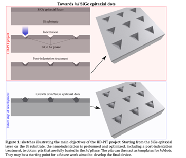
The HD-PIT project aims to understand and engineer the processes inducing a phase transition from the diamond cubic (dc) into the hexagonal diamond (hd) phase by nanoindentation of SiGe layers epitaxially grown on Si wafers. The final goal is to realize hd SiGe pits in the films, which could be subsequently used as a template for the realization of hd SiGe epitaxial dots.
Silicon technology drives phenomenal advances in nano-electronics, but the indirect nature of Si bandgap hinders exploitation for photonic integrated circuits. Interestingly, theoretical studies have shown that the hd phase of SiGe, with a relatively high Ge content, turns the alloy into a direct bandgap material. Recently, SiGe with the hd structure has been obtained by epitaxial growth on III-V nanowires. Confirming the predictions, a direct bandgap has been demonstrated. Despite the high potential of these polytypes for photonics, the present synthesis approaches are not fully compatible with Si technology. Another approach based on pressure-induced phase transition has been exploited, obtaining occasionally the Si and Ge hd phase by nanoindentation. However, a clear control of the hd phase appearance in this context is still lacking neither it is verified for SiGe alloys.
The project will explore the possibility to realize a controlled and extended transition to the hd phase by nanoindentation of Ge-rich SiGe films, being an optimal solution to obtain desired electronic properties in a system fully integrated into the Si platform. A synergic approach leveraging multiscale atomistic simulations, micro-Raman and electron microscopy experiments, will be used for a rational design of the nanoindentation experiments. In fact, it will allow for an efficient search through the large parameter space that includes a wide range of nanoindentation conditions and many different characteristics of the SiGe films. Because of the high Ge content of the SiGe films, they will be grown under strong out-of-equilibrium conditions on Si substrate by low-energy plasma-enhanced chemical vapour deposition (LEPECVD). While Raman micro-spectroscopy and transmission electron microscopy will be used to assess the formation of the hd phase, the multiscale atomistic simulations will guide the experiments. They will involve first-principle calculations of the electronic, structural, and thermodynamic properties of the hd compounds at the atomic scale, but also larger-scale classical molecular dynamics simulations of the whole indentation process, exploiting state-of-the-art interatomic potential based on machine learning approaches. The project will provide fundamental knowledge to boost the monolith integration of hd group IV compounds for on-chip optical components, such as nano-laser and optical amplifiers, thus enabling optical network-on-chip and being breakthroughs for quantum computing, high performance and green ICT.
Objectives
The main goal of the HD-PIT project is to obtain nano-pits fully buried in the hd phase of SiGe, whose transformation from the initial epitaxial dc SiGe layer has been induced by nanoindentation and/or post-indentation treatments. The pits, having both depth and lateral dimensions of a few hundreds of nanometers, may serve as templates for the growth of epitaxial dots made of SiGe with the hd phase. To stay within the proposed timeframe of the PRIN projects, this last target is not pursued in the HD-PIT project but will be the first step of a future and extended project, with the final aim to build a prototype device. In this respect, the HD-PIT will favor the participation of the research units in other initiatives, particularly within EU-Framework programs, to further develop the proposed approach.
Still, the HD-PIT project includes pioneering and challenging objectives:
- Optimize the composition, crystallinity and defectivity of the SiGe epitaxial layer to boost the dc-to-hd phase transition.
- Find the best conditions for the nanoindentation, including temperature, tip shape and orientation, pressure and loading rate to maximize the SiGe volume transited to the hd phase.
- Elaborate a post-indentation treatment to further increase the volume of the initial hd core, allowing it to extend up to the surface of the pits, which should finally be fully buried in the hd phase.
- Define a protocol for the systematic formation of hd SiGe by nanoindentation, particularly aimed at the creation of pits serving as templates for hd SiGe.
All the SiGe layers will be deposited on Si substrates to ensure future compatibility with integrated silicon photonic technologies. The deposited Si1-xGex will have a high Ge content (x>0.70) for two main reasons: firstly, this will ensure a direct bandgap of the hd Si1-xGex formed by nanoindentation if directly exploited for the optically active component; secondly, this will eliminate the lattice mismatch between the substrate and the overgrown dots, when the pits will be used as templates for the hd SiGe epitaxial dots. Additionally, Si and Ge crystals have shown different responses to the nanoindentation. Although further experimental and theoretical confirmations are necessary, their different behavior can be simplified by the fact that, upon loading/unloading, dc Si transform more easily into the r8/bc8 phases (via the β-tin phase), but then a transition from the r8/ bc8 to the hd phase is not happening at room temperature, but only after annealing at a higher temperature, and transition conditions have not a general consensus in the literature. On the contrary, different relaxation pathways were observed by loading/unloading the dc Ge crystals: nucleation of dislocation and twin, and phase transition including the formation of the r8 phase. So, in Ge it is more difficult to obtain phase transition due to the other competing mechanism but, on the other hand, Ge has the advantage of having the r8 phase unstable at room temperature and it seems to transform completely into the hd phase. Thus, the SiGe alloys might be also used to combine and take advantage of the two different behaviors. Besides, nanoindentation on pristine Si and Ge wafers will be performed to compare their response to the nanoindentation and that of the epitaxial SiGe (and pure Ge) layers. Theory-driven experiments will be also performed after the first nanoindentation to possibly expand the formed hd core and to get pits fully buried into the hd phase. This will include thermal treatments and/or a second cycle of nanoindentation.
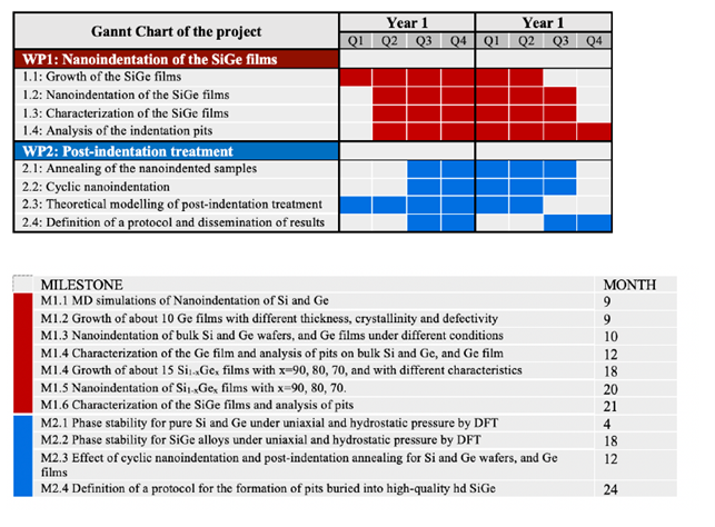
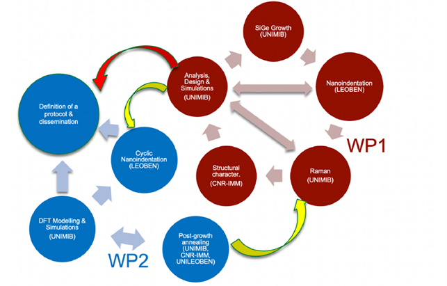
Work Packages & Milestones
Dissemination
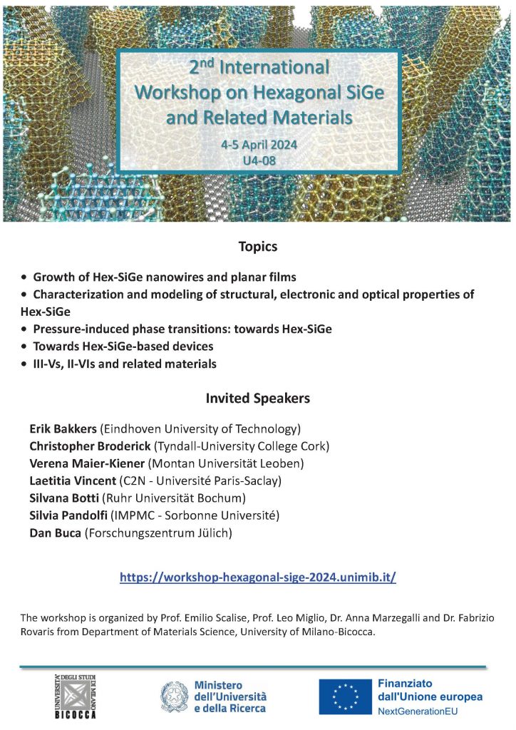
- 2nd International Workshop on Hexagonal SiGe and related materials
- Seminar Prof. Scalise @
- Seminar Dott. Mio @
- Conference Prof. Scalise
- F. Rovaris, A. Marzegalli, D. Lanzoni, G. Ge, A. Fantasia, E. Scalise, F. Montalenti, “Atomic-scale modeling of the pressure-induced dc-hd Phase Transition” in FAME-II Workshop, Eindhoven (Netherlands) 8-9 July 2024
- F. Rovaris, A. Marzegalli, D. Lanzoni, G. Ge, A. Fantasia, F. Montalenti, E. Scalise “Unravelling Atomistic Mechanisms of Pressure-Induced Phase Transitions in Silicon Nanoindentation” in Research at High Pressure – GRS Seminar, Holderness School (New Hampshire) 13-14 July 2024.
Publications
- G. Guojia, F. Rovaris, D. Lanzoni, L. Barbisan, X. Tang, L. Miglio, A. Marzegalli, E. Scalise, F. Montalenti. Silicon phase transitions in nanoindentation: Advanced molecular dynamics simulations with machine learning phase recognition. Acta Materialia. 2024 Jan 15;263:119465. https://doi.org/10.1016/j.actamat.2023.119465
- A. Fantasia, F. Rovaris, O. Abou El Kheir, A. Marzegalli, D. Lanzoni, L. Pessina, P. Xiao, C. Zhou, L. Li, G. Henkelman, E. Scalise, F. Montalenti. Development of a machine learning interatomic potential for exploring pressure-dependent kinetics of phase transitions in germanium. The Journal of Chemical Physics. 2024 Jul 7;161(1). https://doi.org/10.1063/5.0214588
- F. Rovaris, A. Marzegalli, F. Montalenti, E. Scalise. Unraveling the Atomic-Scale Pathways Driving Pressure-Induced Phase Transitions in Silicon. arXiv preprint arXiv:2408.12358. 2024 Aug 22. https://doi.org/10.48550/arXiv.2408.12358
- M. Bikerouin, A. Marzegalli, D. Spirito, G. J. K. Schaffar, C. Bongiorno, F. Rovaris, M. Zaghloul, A. A. Corley-Wiciak, L. Miglio, V. Maier-Kiener, G. Capellini, A. M. Mio, E. Scalise. Formation of Micrometer-Sized Textured Hexagonal Silicon Crystals via Nanoindentation. arXiv preprint arXiv:2410.08372. 2024 Oct 10. https://doi.org/10.48550/arXiv.2410.08372
