Hexagonal Si and Ge and template assisted phase control
Because of the small difference between the gaps in Γ and L points, the Ge band-related characteristics can be tuned via strain engineering. However, efficient light emission has not been fully achieved in this pathway. Instead, it has been realized by exploiting the metastable hexagonal crystal structure that naturally holds a direct band gap for Ge and Ge rich-SiGe alloys. Hexagonal Ge has been obtained via two pathways: as shell material epitaxially grown around almost lattice-matched wurtzite (GaAs) nanowires or inducing phase transition from cubic Ge by high pressure indentation. Extended defects are observed in the new realized crystal structure around nanowires even if no lattice mismatch is present there. Our research team study this previously unknown planar defect and investigate its structural and electronic properties in strict collaboration with the growers at Eindhoven University of Technology. The obtainment of Hexagonal germanium via nanoindentation has been reported in literature, however the systematic and controlled phase transition conditions are not yet identify. Even in this field we are operating with experimental partners (Montanuniversität Leoben, IHP Leibniz Institute for High Performance Microelectronics and CNR-IMM Institute for Microelectronics and Microsystem) modeling the phase transition processes and simulating the indentation. This activity is funded by the Italian ministry as a PRIN-PNRR project named SiGe Hexagonal Diamond Phase by nanoIndenTation (HD-PIT) that Prof. Scalise won as Principal Investigator.
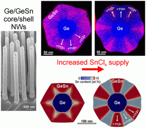
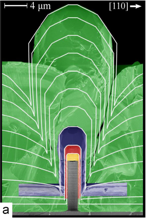
III-V nanowires: morphology, composition and defects
Ga2O3
3C-SiC: growth strategy and defect analysis
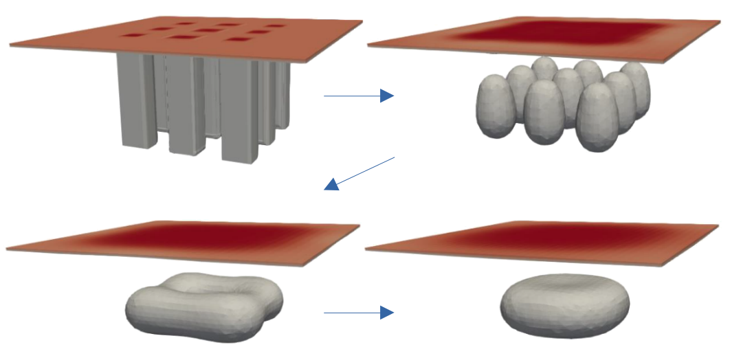
Three-dimensional hetero-epitaxy: growth modeling at the mesoscale
Porous structures