Research topic
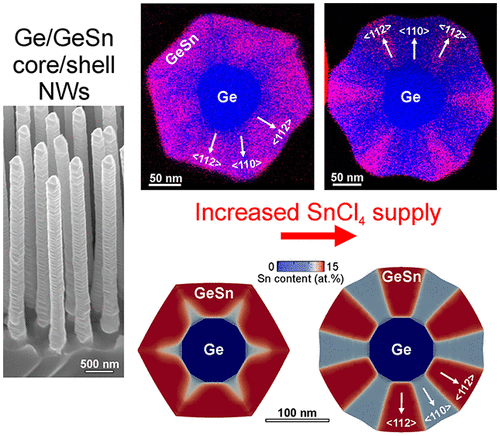
Integration of materials with superior optical and/or electronic properties on Si is extremely appealing as it leads to a wealth of new possible devices and applications while maintaining mainstream silicon technology. Examples include Ge, SiGe, GeSn, SiC, and GaAs. Heteroepitaxial growth of such materials results from the competition between several different phenomena, mostly related to lattice mismatch (causing misfit stress accumulation), to differences in thermal-expansion coefficients (leading to thermal stress), and to kinetic constraints (out-of-equilibrium growth). It is particularly critical for various applications to control the morphology of the growing material (faceting, preferential growth directions, etc.) and the distribution of defects (dislocations, stacking faults, etc.), especially when the 3D growth on patterned substrate is approached. As the growth conditions pertain to a multi-dimensional space, too complex to be sampled by simple trial and error procedures, simulations and modelling can be extremely helpful in driving experiments. Our group provides such theoretical/computational support, aiming at suggesting to experimental colleagues ideal growth conditions for the desired application. Our attention is devoted to a wide class of qualitatively different systems such as semiconductor thin films, quantum dots, nanowires, vertical membranes, and micrometric crystals on deeply patterned substrates.
Open research lines of MoSe group
Computational methods
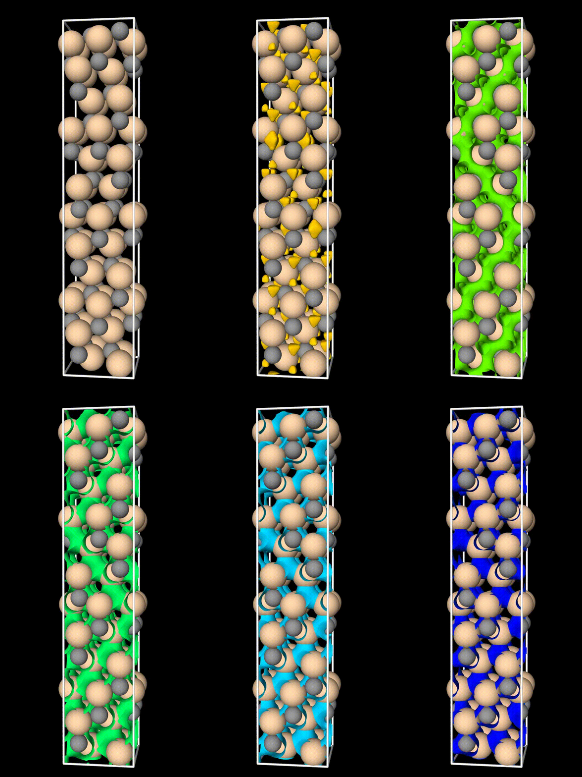
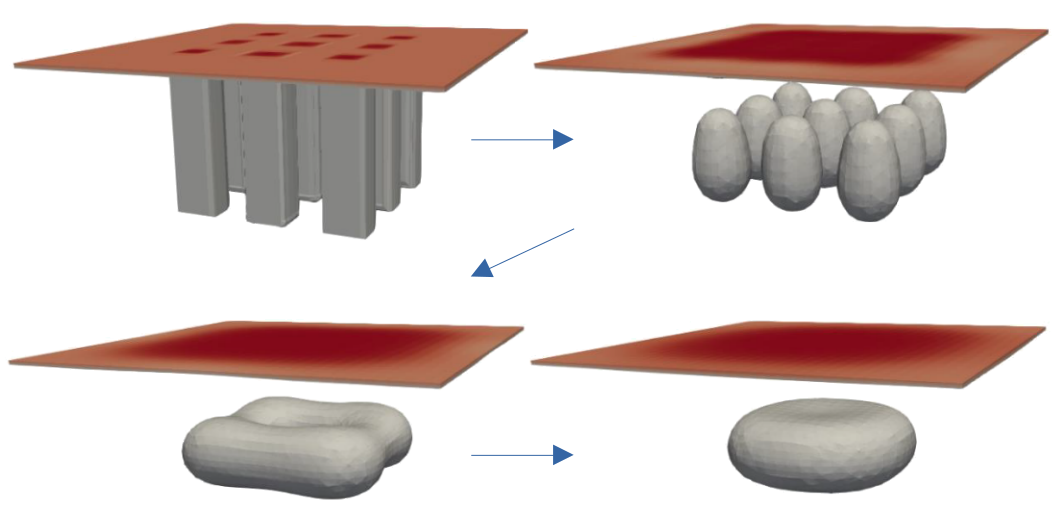
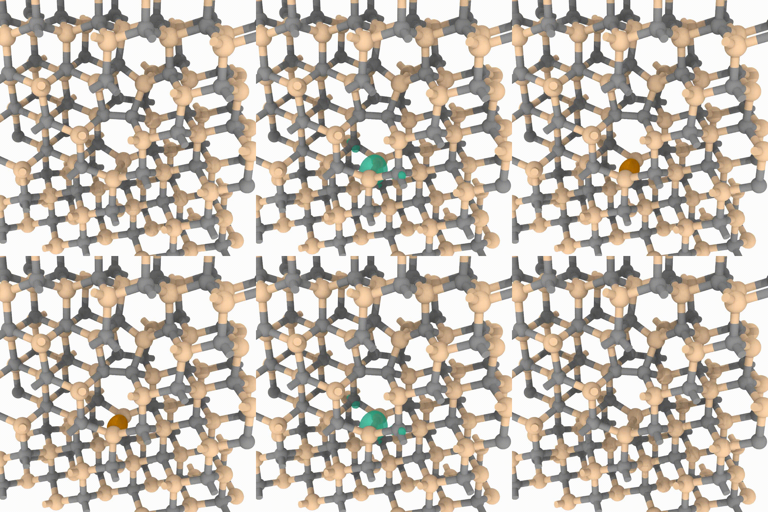
As problems related to heteroepitaxy are often multi-scale, we use different, synergic approaches, ranging from atomistic to continuum simulations. These include ab initio calculations (exploited to evaluate surface energies, diffusion constants, defect formation energy, etc. ), classical molecular dynamics (defect motion, dislocations gliding/partialization etc.), 3D dislocation dynamics, growth simulations based on phase-field methods, and elasticity theory solved by Finite Element Methods.


